Abstract:
Dynamic random-access memory (DRAM), which represents 99% of random-access memory (RAM), is fast and has excellent endurance, but suffers from disadvantages such as short...
View more
Metadata
概要:
ランダムアクセスメモリ(RAM)の99%を表すダイナミックランダムアクセスメモリ(DRAM)は高速で優れた耐久性を備えていますが、データ保持時間が短い(揮発性)、読み取り中のデータの損失(破壊的な読み取り)。結果として、永続的なデータ更新、エネルギー消費の増加、パフォーマンスの低下、スケーリング能力の制限が必要になります。したがって、次世代のRAMは不揮発性RAM(NVRAM)であり、消費電力が低く、耐久性が高く、高速で、非破壊的に読み取られることが望ましいです。ここでは、NVRAMの新しい形式について報告します。それは、その動作上の利点のために量子現象を利用する化合物半導体電荷蓄積メモリです。シミュレーションによると、デバイスの消費電力は非常に小さく、DRAMの単位面積あたりのスイッチングエネルギーは100倍低く、しかし、同様の動作速度で。InAsとAlSbの異常なバンドオフセットにより非揮発性が達成され、大きなエネルギーバリア(2.1 eV)が提供され、電子の漏れを防ぎます。シミュレーション結果に基づいて、書き込みと消去に使用される量子力学的共鳴トンネル機構の結果として、非常に低い妨害率が予測されるNVRAMアーキテクチャが提案されています。
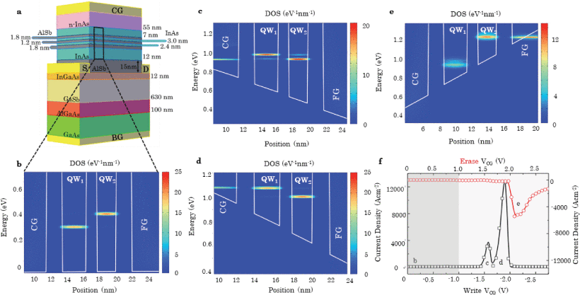
電子メモリの生産と販売は、ダイナミックランダムアクセスメモリ(DRAM)とフラッシュによって支配されています。DRAMは、現在の電子機器のアクティブメモリの主力製品です。生産が速くて安価で、耐久性が非常に高いです。ただし、これにはいくつかの不便な特性、特に揮発性と破壊的な読み取りもあります。その結果、持続的なデータ更新が必要になり、帯域幅、スケーリング容量、メモリのエネルギー消費に悪影響を及ぼします[1]。その結果、DRAMのすべての利点を備え、「ユニバーサルメモリ」と呼ばれることもある欠点のない代替メモリの概念の探索が続けられています。ユニバーサルメモリセルは、不揮発性、低電圧、低エネルギー、非破壊読み出し、安価、高速、高耐久性である必要があり、すべてのメモリ要件に対応するユニバーサルソリューションを提供します。たとえば、このようなメモリを不揮発性RAM(NVRAM)として実装すると、コンピューティングのパラダイムシフトが生じます。しかし、一見克服できないつまずきのブロックは、非常に堅牢なプログラム状態を必要とする非揮発性の見かけ上矛盾する要件と、容易に変更できる状態を意味する高速の低電圧(低エネルギー)書き込みおよび消去を備えています。[2]。 ここでは、トリプルバリア共鳴トンネル(RT)構造の量子特性を活用して、不揮発性と低電圧の書き込みおよび消去の矛盾した組み合わせを可能にする新しいメモリ[3]について報告します。大きな(2.1 eV)障壁のため、InAs / AlSbシステムの固有(熱励起)電子蓄積時間は、宇宙の年齢を大幅に超えると予測されていました[4]。明らかに、実際のデバイスでは、他の損失メカニズムが存在すると、実際のストレージ時間が劇的に短縮されます。それにもかかわらず、2.1 eVの障壁はNANDフラッシュ(1.6 eV)の障壁を超えるため、このようなデバイスは不揮発性であることが期待され、これは最近の研究で実証されています[9]。それにもかかわらず、書き込みと消去には≤2.3Vが必要です。ここで詳述するシミュレーション結果は、商用ソフトウェアの組み合わせを使用して実装された特別に開発された室温モデルからのものです。nextnano多重散乱ブッティカー(MSB)ソフトウェア[5]、[6]は、RT構造(書き込みおよび消去)、チャネルをモデル化するためのnextnano ++(読み取り)、および集積回路によるシミュレーションプログラムを介したキャリアの輸送を調査するために使用されました対応する全体的なデバイスおよび回路レベルのプロパティを決定するための強調(SPICE)[7]。デバイスの物理をモデル化するために使用されるシミュレーションパラメーターは、表Iで提供され、実験的に観測された定数[6]、[8]に固定されています。デバイスの選択された構造は、室温で低電圧で動作するごく最近報告されたメモリセルに基づいています[9]。これらのデバイスでは、読み取りプロセスで「通常オン」の空乏モードチャネルを使用しました。つまり、ゼロゲートバイアスで導通しています。ただし、これは、アドレス指定されていないアレイ内のデバイスをオフに切り替えることができないため、RAMへの実装を禁止します。ここでは、この障害を克服するために、読み取りサイクルに使用されるチャネルの厚さを減らして量子井戸(QW)を形成し、量子閉じ込めを利用して、デバイスを読み取るための導電性のしきい値電圧を持つチャネルを作成します。この構造適応により、動作可能なフローティングゲート(FG)RAMに必要な「通常はオフ」のチャネルが生成されます。RTシミュレーションの結果とQWチャネル(QWCH)SPICEプログラムへのシミュレーションは、このメモリがDRAM速度で妨害のない完全に機能するRAMとして動作できることを予測していますが、不揮発性と非破壊読み出しの追加の利点があります。 装置の構造を図1(a)に模式的に示します。このメモリの特徴は、薄いInAs / AlSb層で構成されたトンネル接合で、トリプルバリア構造を形成することです。トンネル接合の重要な特徴は、ゼロバイアス下では電子が通過できないことですが、コントロールゲート(CG)とチャネル間の小さな電位(≤2.3V)で電子が通過できることです。小さい特定の電圧範囲(〜0.5 V)内で、電子はジャンクションを介してRTを介してFGに(またはFGから)急速に輸送されます。これにより、シャープで高い電流密度のピークが得られ、メモリが不揮発性とRAM機能を実現できるようになります。このプロセスを理解し、この領域を通る輸送をシミュレートして、デバイスのパフォーマンス特性を調査することが重要です。
FGは、トンネル領域を形成する薄いAlSbバリアをトンネリングする電荷を保存する電子閉じ込め層です(図1(a)を参照)。フラッシュメモリで使用されるFG金属酸化物半導体電界効果トランジスタ(FGMOSFET)セルと同様に、状態を定義するのはこの電荷蓄積領域です[9]。論理「1」は、FG内に電荷がない状態に割り当てられます。適切な電圧パルスが印加されると、電荷はCGからFGへ量子的に機械的にトンネルし、そこでAlSb電荷ブロッキング層によってトラップされます。この状態は、FGに電荷を追加する(書き込みサイクル)ことによって達成される論理「0」として定義されます。同様に、反対極性の電圧パルスを使用して、FGから電荷を除去し、「1」状態に戻すことができます(消去サイクル)。[3]、[9]。 トンネル領域の三重障壁構造は、構造内に2つのQWを形成し[ 図1(b)を参照 ]、電子を異なるエネルギーレベルに閉じ込めます[9]。従来のトンネリング(つまり、共鳴状態ではない)による漏れを防ぐために十分に厚い障壁を生成するには、2つのQWが必要です。同時に、薄いQWを使用すると閉じ込め状態が上がり、明確なRTピークが生成されます。さらに、ウェルの厚さは、2つのウェル間のエネルギー状態の整合を防ぐのに十分に異なるため、さもなければ中央障壁の電子阻止能力が低下します。トンネル接合の両端に電圧を印加すると、伝導帯が傾斜し、入射電子(エミッター)のエネルギーに対するエネルギーレベルが変化します。この構造の場合、トンネル接合の外側の電子は、印加電圧から三角形のウェルが形成されるため、準束縛状態になります[11]。。これは、図1(c)および(d)に表示されている書き込みプロセスの状態密度(DOS)のカラースケールで示されています。これらの図では、伝導帯はデバイスのCGに印加された電圧に起因する勾配にあります。図1(e)に示すように、反対の極性の電圧を使用して、同様のDOSプロットを消去プロセスに使用します。 コヒーレントRTにより、ウェルのエネルギーレベルがフィルターとして機能し、同様のエネルギーを持つ電子のみが透過します。バイアスをかけると、エミッタからの入射電子のエネルギーに対してウェル状態のエネルギーレベルが低下します。これは、ソース、つまり書き込みサイクルのCGでの電子の準束縛状態であり、FG消去サイクル用。特定の印加バイアスでは、入射電子のエネルギーとAlSbバリアの反対側のウェルのエネルギーレベルは同じであるため、バリアを通過する透過率が急激に増加します。バイアスが印加され、エミッタのエネルギーがQWエネルギーを超えると、バリアを通過する透過率が急激に低下します[12]。これは、図1(f)のデバイスのトンネル接合の電流密度プロットで示されています。ここで、印加電圧はデバイス端子間にあります(つまり、15 nm AlSbバリアが考慮されます)。結果は、書き込みプロセスの負のCGバイアス下のトンネル接合の2つの鋭い電流ピークを示しています。-1.6 Vに小さいピークは、QW用エミッタウェルエネルギーアライメントの特徴である2 QWの電子波動関数(FG最寄りQW)、2はまた、QW内の空間に存在する1、トンネル接合の第一ウェル[ 図1(c)を参照 ]。これにより、QW 1およびQW 2を介したCGからFGへのトンネリングが可能になります。高速で一貫したプロセスで。同様に、高電圧(-1.9 V)での2番目の大きなピークは、準束縛エミッターのエネルギー状態とQW 1のエネルギーの整合によるものです(図1(d)を参照)。図1(f)でcおよびdのラベルが付けられたDOSプロットのバイアスは、書き込みプロセスのトンネル電流のピークに対応し、書き込みサイクルの電流と電圧の関係がコヒーレントRTの結果であることを示していますQW 1とQW 2を組み合わせたエネルギー配列からのInAs / AlSbトリプルバリア構造。 トンネル接合のシミュレーションは、消去サイクルに逆極性の電圧を使用して繰り返されました。結果は書き込みサイクルに似ており、FG電子エネルギーに対応する電流ピークがトンネル接合のQWエネルギーと一致しています[ 図1(e)を参照 ]。ただし、2つのQW状態間のエネルギーの違いにより、ピークはより高い印加バイアスにシフトします[ 図1(b)を参照 ]。これは、InAsウェルQW 1とQW 2の幅が異なる(3.0それぞれ2.4 nm)。この結果、消去電圧は書き込み電圧よりも高くなります。 結果として生じる電流ピークは、低電圧(≦2.3 V)でFGに電子が出入りできること、およびゼロ電圧で流れる電流がゼロであることを示しています。したがって、トンネル接合は電荷蓄積メモリデバイスアプリケーションに対して効果的に動作します。これは、印加バイアスが除去されるとバリアを通るリーク電流がなく、適切な書き込み(または消去)バイアスが印加されると大きな電流密度が発生するためです。0 Vで電流密度がなく、±1 Vまでの非常に小さい<1 Acm -2の電流密度は、InAs / AlSbシステムの2.1 eVの障壁の高さから予想される良好なデータ保持を示しています。 このプロセスのシミュレーションにより、これらの結果を別のモデル(SPICE)に転送して、図1(f)の電流密度の関係を使用して、メモリデバイスのパフォーマンスベースの特性を特徴付けることができます。電流密度の結果からの重要な認識は、ピークの鋭さから直接見られ、ピークから離れた電圧での非常に小さな電流(<1 Acm -2)である[ 図1(f)を参照]]。これにより、書き込みと消去のサイクルに必要な電圧をCGとチャネル(ドレインDとバックゲート(BG)を接地)に分割し、それらを組み合わせて目的の書き込みまたは消去サイクルを実行できます。重要なのは、これらの半分の電圧のいずれかを適用しても、セルの論理状態が変更されないことです。後で、これによりRAMのアーキテクチャを実現する方法を示します。 メモリチップに保存されているデータを読み取るには、大きなアレイ内の個々のデバイス(ビット)の論理状態を判断できる必要があります。フラッシュメモリでは、チャネルが絶縁状態から導電状態に移行するCGのバイアスとして定義されるしきい値電圧を使用して、デバイスレベルの読み出しが実現されます。デバイスのFGに電荷が追加されると、CGでデバイスに印加される電位が部分的にスクリーニングされます。これにより、しきい値電圧がより大きな値にシフトし、電圧シフトの大きさはΔ VT= QF GCF G(1)
ソースを見る \begin{equation*} \Delta V_{T} =\frac {Q_{\mathrm {FG}}}{C_{\mathrm {FG}}}\tag{1}\end{equation*}
どこ CF G
CGとFGの間の静電容量(平行平板近似から計算される 1.2 μ
デバイスのFcm -2)およびQF G
FGに保存されている電荷です[14]。両方として注意してくださいQF G
そして CF G
断面積に直接比例するため、上記の式から削除されます。これにより、しきい値電圧シフトの1次元方程式が生成され、ここで使用される厳密な1次元シミュレーションが正当化されます。 \begin{equation*} \Delta V_{T} =\frac {Q_{\mathrm {FG}}}{C_{\mathrm {FG}}}\tag{1}\end{equation*}
どこ CF G
CGとFGの間の静電容量(平行平板近似から計算される 1.2 μ
デバイスのFcm -2)およびQF G
FGに保存されている電荷です[14]。両方として注意してくださいQF G
そして CF G
断面積に直接比例するため、上記の式から削除されます。これにより、しきい値電圧シフトの1次元方程式が生成され、ここで使用される厳密な1次元シミュレーションが正当化されます。 しきい値電圧シフトは、FG(0)に電荷が存在する場合のデバイスと比較して、FG (1)に電荷が存在しない場合にメモリデバイスに異なるしきい値電圧が存在するシステムを作成します。これら2つのしきい値の違いにより、しきい値電圧ウィンドウ(Δ VT
)[15]、その中に基準電圧(VR E F
)デバイスの論理状態を判断するには:論理1(印加電圧がしきい値を超える)の場合、チャネルは導通し、論理0(印加電圧がしきい値を下回る)の場合は非導通になります。ここでは、同様の読み取り手法を使用することを提案します。このデバイスのしきい値電圧は、CGとBGの間に電圧を印加することにより生成されます。ここで示すシミュレーションでは、デバイスに12 nm-In 0.8 Ga 0.2 Asチャネルを使用します[ 図1(a)を参照 ]。ただし、他の組成と厚さでも同様の効果が得られます:5 nmのInAsまたは14 nm In 0.7 Ga 0.3のたとえば、これにより、しきい値電圧が生成され、これにより、個々のデバイスの論理状態を大きなアレイ内で読み取ることができます。この変更は、以前のサンプルと比較してデバイスの全体的な歪みも低減します[9]。チャネル層の厚さの大幅な減少は、ガリウムの小さな組成の導入による格子不整合の増加を補償します[16]。 チャネルはQW(QW CH)を形成します。これにより、隣接するGaSbの価電子帯エネルギーよりも電子占有の最小エネルギー要件が高くなります[ 図2(a)を参照 ]。その結果、CGのゼロまたは低バイアスでは、GaSb価電子帯の電子はQW CHに移動できず、空いている(したがって、絶縁性の)チャネルになります。ポテンシャルの適用(VC G − B G
)CGとBGの間でGaSbの価電子帯が上昇します。GaSb価電子帯の一部がQW CH基底状態エネルギーを超えると、電子がGaSb価電子帯からQW CHに移動し、絶縁状態から伝導状態に遷移します。つまり、トランジション。これは、基準電圧(図2(a)の読み取り操作のシミュレーション結果に示されています(VR E F
)、ここで、In 1-x Ga x As伝導帯によって形成されるQW CH状態[ 図2(a)および(b)緑の一点鎖線] は、GaSbの価電子帯エネルギーよりも部分的に低い(灰色の短い-破線):チャネルは占有され、導電性であり、デバイスはロジック1です。同じ基準電圧のロジック0のセルでは、価電子帯はQW CH基底状態エネルギーの下にあり、チャネルは絶縁されたままです(ピンクの点線)ライン)。
したがって、チャネル内の電子密度、したがって導電率は、CGとBG間の電位の関数です。チャネルの導電率はσ= e n2 Dμ(2)
ソースを見る\begin{equation*} \sigma =en_{2D} \mu\tag{2}\end{equation*}
どこ e
電子の電荷であり、 μ
In 0.8 Ga 0.2 Asチャネル内の電子の移動度です[17]。特定のCG–BG電圧でのチャネルの電子占有率は、2-D DOSを使用して計算されます。したがって、2-Dキャリア密度n2 D= 2 m∗C Hπℏ2Δ E(3)
ソースを見る\begin{equation*} n_{2D} =2\frac {m_{\mathrm {CH}}^{\ast }}{\pi \hslash ^{2}}\Delta E\tag{3}\end{equation*}
どこ m∗C H
は、チャネル内の電子の有効質量です[17]、ℏ
縮小プランク定数、および Δ E
は、GaSb価電子帯とQW CHエネルギー状態の間のエネルギーの重なりです[18]。合成(2)及び(3) (シミュレートエネルギー重複とΔ E
)デバイスの場合(図2(a)を参照)、図2(c)に示すように、デバイスを読み取るための導電率と電圧の関係を直接取得できます。 フラッシュテクノロジーと同様に、FGに電荷を追加すると、デバイス全体の電位(この場合はCG–BG電位(VC G − B G
)。これにより、図2(c)のピンクの点線で表される(1)に従って、書き込みサイクル中に導電率-電圧曲線全体がより高い電圧にシフトします。同様に、FGから電荷が除去されると、消去サイクルにより関係が元の状態に戻ります。Flashテクノロジを使用した読み取り技術の類似性は、デバイスがRAMとしてどのように機能するかには関係ありません。実際、同様の読み取り手法を使用すると、複数のデバイスのアレイを組み立てながら、シングルビットアクセスも可能になります。このメモリをNVRAMとして動作させるのは、トリプルバリアRTメカニズムです。 SPICEプログラム(ltSPICE)を使用して、ソフトウェアパッケージnextnano.MSBおよびnextnano ++ [7]を使用して作成された書き込み/消去および読み取りシミュレーション結果を組み合わせました。FGメモリの特性評価に使用されているSPICEモデルの例は多数あります[13]、[19]、[20]。ただし、通常は、すでに作成されたデバイスのモデリングに焦点を当て、容量結合係数やトンネリングパラメーターなどの実験測定からモデルの情報を抽出します(トンネリングパラメーターもモデル化できます[20])。これらは、その後、実験データと直接比較するためにシミュレーション中に挿入されている[19] 、[20]。確立されたモデルまたは実験的に導出されたパラメーターが利用できないこの記事では、トンネリングメカニズムのデータは電圧制御電流源(VCCS)で表され、電流をモデル化します(デバイス領域、At uとn個
)図1(f)のシミュレートされたトンネリング結果への複数のピークを持つ非対称ガウス近似から。結果は、トンネル領域に印加される電圧に依存します。トンネル領域の両端の電圧は、書き込みおよび消去プロセス中の2つのバイアス、CG電圧とソース(S)電圧から発生します。トンネル領域全体の結合バイアスは、CGとSの両方から電圧を印加したデバイスの拡張nextnano ++シミュレーション用のポアソン-シュレディンガーソルバーを使用して、バンド構造勾配(およびRTアライメント)の個別の調査から決定されます。接点間の電圧とデバイスのトンネル領域で見られる電圧との間。図1(f)CG電圧のみのこれらの補正が既に含まれています。これにより、容量結合近似よりも正確であると思われるトンネル電圧の物理モデルが得られます[20]。 さらにnextnano ++を使用して、高度にドープされた(n +)CG層のバンドベンディングの影響をさらに調整します。また、書き込みまたは消去プロセス中に変化するFG上の電荷の存在による電圧スクリーニング効果も考慮する必要があります。したがって、VCCSによって供給される電流は、独自の電流出力が入力電圧を遮断するにつれて変化します。書き込みパルスおよび消去パルス中のFGの電荷の増加または消失。 このシステムをモデル化する最も簡単な方法は、上記のすべての情報を含むVCCSを容量のあるコンデンサに接続することです CT
、トンネル接合と電荷ブロッキングバリアからFGに結合された総静電容量(平行平板近似から計算される 2 μ
Fcm -2 ; 図3を参照)。電圧パルスが印加されると、トンネル接合の両端の電圧に変換され、そこからVCCSは図1の RTシミュレーション結果に従って応答し、FGの変化する電荷を継続的に考慮するように電流を放出します。書き込みプロセスで放出された電子は、FGコンデンサに保存され、電圧VF G 1
作成されます(図3を参照)VF G 1= QF GCT。(4)
ソースを見る\begin{equation*} V_{\mathrm {FG}1} =\frac {Q_{\mathrm {FG}}}{C_{\mathrm {T}}}.\tag{4}\end{equation*}
この結果は、電圧スクリーニング効果としてVCCSにフィードバックされます。同様に、このセットアップは、FG(消去)から出る電荷をシミュレートするために使用できます。初期電圧は、VI N I T I A L
、デバイスの以前に書き込まれた状態を定義します。(1)と(4)を材料の層厚と誘電率を使用して平行平板コンデンサとして近似したデバイスの静電容量と組み合わせると、チャネルのしきい値電圧シフトの式を次の関数として取得できます。VF G 1
、 あれは Δ VT= CTCF GVF G 1。(5)
ソースを見る\begin{equation*} \Delta V_{\mathrm {T}} =\frac {C_{\mathrm {T}}}{C_{\mathrm {FG}}}V_{\mathrm {FG}1}.\tag{5}\end{equation*}
その結果、過渡シミュレーションで任意の電圧パルスのしきい値シフトを追跡し、セクションIVで説明したチャネルの導電率関係の変化を判断できます[ 図2(c)を参照 ]。
ここで報告するデバイスとフラッシュメモリセルの類似性により、フラッシュアーキテクチャとの互換性が容易になります。つまり、デバイスを大きな文字列で直列に接続したNAND型アーキテクチャで実装できます。これにより、NANDフラッシュに代わる低消費電力の高耐久性が可能になります。ただし、大規模な使用には、平面から3D NANDフラッシュへの移行に対抗するために、3D実装と面積ビット密度の増加が必要になります。代替手段は、高ビット密度のFGMOSFETベースのフラッシュメモリよりも信頼性の高いデータ保持、高速、低エネルギーが望ましいニッチアプリケーションでの使用です。 さらに興味深いのは、アクティブメモリ(RAM)に適したアーキテクチャでの実装です。アクティブメモリの最も重要な機能は、ユーザーのコマンドで個々のビット(デバイス)に高速アクセスできることです[21]。私たちのデバイスでは、これはNORタイプのアーキテクチャを実装することで実現できます(図4を参照)。図4に、よく知られているFGMOSFETデバイスシンボルに似ているが、書き込み/消去メカニズムを指定するためのRTダイオードシンボルと組み合わせた新しいデバイスシンボルを紹介します。RTの性質により、書き込みおよび消去プロセスの電流ピークは非常に鋭くなります[ 図1(f)を参照]]。これにより、データの書き込みまたは消去に必要な電圧の半分がCGに、残りの半分がチャネルに適用される、半電圧の使用が可能になります。単一の半電圧のみがデバイスに適用されると、デバイスの状態はそのまま残ります。この機能を使用して、CGおよびSとしてそれぞれ指定する目的のワードラインおよびビットラインで半電圧を選択することにより、アレイ内の個々のデバイスをターゲットにできます。これらを組み合わせて、周囲のデバイスに保存されているデータを損なうことなく、ターゲットデバイスの書き込みまたは消去を行います(妨害)。BG端子はアレイ内のすべてのデバイスの共通グランドとして機能し、デバイスは接地ドレイン接点とペアで背中合わせになり、非常に効率的なアーキテクチャを可能にすることに注意することが重要です(図4を参照)。
その他の点では、読み取り操作はNORフラッシュメモリで見られる操作と同じであり、このアーキテクチャで個々のデバイスの読み取りを許可します[22]。これは、読み取り電圧を印加することにより達成されます。VR E F
、CGとBG(CGとグランド)の間、適切なワードライン、適切なビットラインに小さな電圧、たとえば<0.5 V、およびチャネル伝導度(電流)をテストします。デバイスは通常オフであるため、アドレス指定された特定のデバイスが論理1状態にある場合にのみ電流が流れることに注意してください。VR E F
0と1の状態の2つのしきい値電圧、たとえば0.6 Vの間に収まるように選択する必要があります[ 図2(c)を参照 ]。個々のデバイス(ビット)をターゲットにする機能は、個々のビットをランダムにアドレス指定する速度のため、RAMアプリケーションに向いています。主要なRAM技術であるDRAMとは異なり、このメモリは非破壊読み取りで不揮発性ですが、他の点では同様の(または改善された)パフォーマンス機能を備えています。 モデリングは、そのようなNVRAMが低電圧、低エネルギー、高速で動作できることを示しています。立ち上がり時間が5ナノ秒、持続時間が5ナノ秒の書き込みサイクルの過渡シミュレーションを、デバイスの潜在的な速度を示して図5(a)に示します。これにより、DRAMの速度と同様に、合計パルス時間が10 nsになります[23]。。しきい値シフトの立ち上がり時間とパルスの持続時間の両方に依存しています。したがって、デバイスの速度を調査するために、それらは等しく設定されました。5nsの立ち上がり時間の電圧パルスは、特にDRAMを考慮して選択されました。この速度制限は、メモリアレイ内の容量性充電の結果です。したがって、電圧パルスの選択では、仮想アレイの実装によってもたらされる容量制限を考慮します。この図は、パルス中のリアルタイムでのしきい値電圧の変化と、対応するトンネル電流密度、つまり書き込みパルス中にFGにトンネルする電流密度を示しています[ 図5(a)を参照]]。したがって、FGに保存される電荷密度はこのプロットの下の面積であり、(1)に従ってしきい値電圧が変化する唯一の理由です。図5(b)は、消去サイクルの同じプロットを示しています。同じサイクルではなく、同様の速度と電圧で動作しています。つまり、現在説明しているように、電流密度曲線の下の面積が等しくなります(図5を参照)。
4つの最適化された半電圧パルスは、-0.85 V(CG書き込み)、0.90 V(S書き込み)、-1.16 V(S消去)、および1.16 V(CG消去)です。書き込みおよび消去サイクルの合計電圧は、ピーク電流密度に対応する電圧よりわずかに大きくなります[ 図1(e)を参照 ]。これは、電圧の変化によるものですVF G 1
書き込みおよび消去プロセス中に、印加電位の一部をスクリーニングし、わずかに高い電圧で補償する必要があります。書き込みまたは消去プロセスのしきい値シフトが正反対になるように、書き込みまたは消去の各ビットラインまたはワードラインに固有の電圧振幅が選択され、多くのサイクルにわたってしきい値電圧にドリフトがないようにします。半電圧は、個別に適用された場合、周囲のセルにほとんど影響を与えません。セル上の最大の妨害は、ワードラインに印加される-0.85-Vの書き込み半電圧によるもので、20 nmのフィーチャサイズで4000 10 nsのパルスごとに約1つの電子損失であると判断されました。セルの非常に低い妨害は、低電圧でのトンネル電流の欠如に由来します。これは、電流密度シミュレーションから直接示されます[参照図1(f) ]、電流密度は0.85〜1.16 Vの範囲で1 Acm -2未満です(ピーク値10 4 Acm -2と比較)。読み取りプロセスでは、モデルは430 mVの優れた0/1しきい値コントラストを予測します[ 図2(c)を参照 ]。 私たちは今、20-nmのフィーチャサイズのセルでメモリセルの異なるタイプの重要なメモリ指標のいくつかを比較する場合は、[23] 、[24]生産中及び開発中の両方、我々はいくつかの興味深い結果を観察(参照表IIを)。最も注目に値するのはスイッチングエネルギーで、DRAMと3-D NANDフラッシュの両方よりもそれぞれ100倍と1000倍低いため、他の新しいメモリテクノロジーよりも大幅に低くなります。この注目すべき観察結果は、デバイスの低電圧と小さな静電容量の組み合わせの結果です。さらに、バリアエネルギーを克服するために必要なエネルギーのために、不揮発性メモリは状態を変更するために揮発性メモリよりも多くのエネルギーを消費する必要があるという議論と矛盾します[23]。。これはRTの場合ではありません。トンネリングが発生する可能性のある非常に特定のエネルギーアライメントのみが存在するため、高いバリアエネルギーを保持しながら、小さな電圧でトンネリングを観察できます。表IIにリストされているベンチマークメトリックで明らかになった唯一の問題は、FGの小さな静電容量の欠点である電子数です。このフィーチャサイズで書き込み状態(0)のFGに100個の電子しかない場合、30〜50個の電子の漏れにより、そのデータセルが故障する可能性があります。ただし、シミュレートされた0 Vリーク電流は300 Kで無視できる程度であり、前述のように、半電圧パルスの乱れは非常に小さくなっています。さらに、同様の機能サイズの2-D NANDフラッシュテクノロジーは、セルレベルあたり30〜50の電子しか持っていません[24]。この比較は、高いバリアエネルギーと低い妨害率と組み合わされて、少なくとも技術が10 nm未満のフィーチャサイズにスケーリングされるまで、この少数の蓄積電子が障害になることはないことを示唆しています。 驚くほど低いスイッチングエネルギー(10 -17J(20 nmフィーチャサイズ))は、フラッシュよりも大幅に低い電圧(≤2.3V)でFGメモリとして動作します。非常に低いスイッチングエネルギーと大きなバリアエネルギー(2.1 eV)により、ポジティブな耐久性とデータ保持の結果が期待されますが、実験デバイスでの厳密なテストが必要です。nextnano.MSB、nextnano ++、およびSPICEシミュレーションの組み合わせは、デバイスが10 nsのパルス持続時間で実質的に妨害なしに動作できることを示しています。これは揮発性の代替DRAMと同じ速度です。これらの利点は、他のFGメモリ(フラッシュなど)よりもはるかに低い電圧で発生する電荷をデバイスに出し入れするために使用されるトリプルバリアRTメカニズムに由来します。提案されたデバイスには、しきい値電圧と、電荷蓄積によるしきい値電圧シフトがあります。フラッシュメモリで使用されるFGMOSFETセルと同様の読み取りプロセスを許可します。これは、Inから形成された壊れたギャップ(タイプIII)伝導バンドアライメントを使用して実現されます。1-x Ga x As / GaSbヘテロ接合。In1 -x Ga x Asチャネルは薄い(12 nm)QWです。0状態と1状態の間のしきい値電圧の優れたコントラストが達成されます。フラッシュメモリセルに類似しているため、NANDまたはNORフラッシュアーキテクチャをデバイスに直接実装して、大きなアレイを作成できます。シミュレーション結果は、NOR型アーキテクチャ内で半電圧を使用して、書き込み、消去、および読み取りプロセスの個々のセルをターゲットにできることを示しています。この独自の機能は、1-Dモデルの過渡結果から示唆される高速化と組み合わされ、DRAMに代わる低電力、不揮発性、非破壊読み取りの代替としてデバイスを大規模アレイに実装できることを予測します。 了承この原稿の図のデータは、[27]のランカスター大学のデータアーカイブから公開されています。
|
Abstract:
Dynamic random-access memory (DRAM), which represents 99% of random-access memory (RAM), is fast and has excellent endurance, but suffers from disadvantages such as short...
View more
Metadata
Abstract:
Dynamic random-access memory (DRAM), which represents 99% of random-access memory (RAM), is fast and has excellent endurance, but suffers from disadvantages such as short data-retention time (volatility) and loss of data during readout (destructive read). As a consequence, it requires persistent data refreshing, increasing energy consumption, degrading performance, and limiting scaling capacity. It is, therefore, desirable that the next generation of RAM will be nonvolatile RAM (NVRAM), have low power, have high endurance, be fast, and be nondestructively read. Here, we report on a new form of NVRAM: a compound-semiconductor charge-storage memory that exploits quantum phenomena for its operational advantages. Simulations show that the device consumes very little power, with 100 times lower switching energy per unit area than DRAM, but with similar operating speeds. Nonvolatility is achieved due to the extraordinary band offsets of InAs and AlSb, providing a large energy barrier (2.1 eV), which prevents the escape of electrons. Based on the simulation results, an NVRAM architecture is proposed for which extremely low disturb-rates are predicted as a result of the quantum-mechanical resonant-tunneling mechanism used to write and erase.
Page(s):
474 - 480
Date of Publication:
01 January 2020
Production and sales of electronic memories are dominated by dynamic random-access memory (DRAM) and Flash. DRAM is the workhorse of active memory in current electronics. It is fast and cheap to produce and has very high endurance. However, it also has some inconvenient properties, notably volatility and destructive read. As a result, persistent data refreshing is required, negatively affecting the bandwidth, scaling capacity, and energy consumption of the memory [1]. Consequently, the search for alternative memory concepts with all the advantages of DRAM and none of the disadvantages, sometimes called “universal memory,” continues. Universal memory cells should be nonvolatile, have low voltage, have low energy, should be nondestructively read, should be cheap, should be fast, and have high endurance, providing a universal solution for all memory requirements. Implementing such a memory as a nonvolatile RAM (NVRAM), for example, would produce a paradigm shift in computing. However, a seemingly insurmountable stumbling block comprises the apparently contradictory requirements of nonvolatility, which necessitates a very robust programmed state, and fast low-voltage (low-energy) write and erase, which implies a state that can be readily changed. This has led to the view that the universal memory concept is not realistic [2]. Here, we report on a novel memory [3] that exploits the quantum properties of a triple-barrier resonant tunneling (RT) structure to allow the contradictory combination of nonvolatility with low-voltage write and erase. Due to the large (2.1 eV) barrier, the intrinsic (thermal excitation) electron storage time of our InAs/AlSb system was predicted [4] to exceed substantially the age of the Universe. Clearly, in real devices, the presence of other loss mechanisms will lower the actual storage time dramatically. Nevertheless, the barrier of 2.1 eV exceeds that of NAND Flash (1.6 eV), so such devices are expected to be nonvolatile, and this has been demonstrated in recent work [9]. Despite this, write and erase require ≤2.3 V. The simulation results detailed here are from a specially developed, room-temperature model implemented using a combination of commercial software. The nextnano multi-scattering Büttiker (MSB) software [5], [6] was used to investigate the transport of carriers through the RT structure (write and erase), nextnano++ to model the channel (read), and Simulation Program with Integrated Circuit Emphasis (SPICE) [7] to determine the corresponding overall device and circuit-level properties. The simulation parameters used to model the device physics are provided in Table I and are fixed to experimentally observed constants [6], [8]. The chosen structure of the device is based on very recently reported memory cells operating at low voltages at room temperature [9]. In these devices, the read process used a depletion mode channel that is “normally ON,” i.e., is conducting at zero gate bias. However, this inhibits its implementation in a RAM, as devices in the array that are not being addressed cannot be switched OFF. Here, to overcome this obstacle, the thickness of the channel used for the read cycle is reduced to form a quantum well (QW), exploiting quantum confinement to create a channel with a threshold voltage for conductivity to read the device. This structural adaptation produces the “normally OFF” channel that is required for an operational floating gate (FG) RAM. Combining the results of the RT simulations and QW channel (QWCH) simulations into a SPICE program predicts that this memory can operate as a disturb-free, fully functional RAM at DRAM speeds, but with the additional advantages of nonvolatility and nondestructive read.
SECTION II. Device ConceptThe construction of the device is illustrated schematically in Fig. 1(a). The memory features a tunneling junction constructed from thin InAs/AlSb layers to form a triple-barrier structure. The key characteristic of the tunneling junction is that it does not allow electrons to pass through it under zero bias, but will under small potentials between the control gate (CG) and the channel (≤2.3 V). Within a small and specific voltage range (~0.5 V), electrons are rapidly transported through the junction via RT to (or from) the FG. This results in sharp and high current-density peaks that allow the memory to achieve nonvolatility and RAM capabilities. It is important to understand this process and simulate transport through this region to investigate the performance characteristics of the device.
The FG is an electron-confining layer that stores any charge that tunnels through the thin AlSb barriers, which form the tunneling region [see Fig. 1(a)]. It is this charge storage region that defines the state, similar to the FG metal–oxide–semiconductor field-effect transistor (FGMOSFET) cells used in Flash memory [9]. Logic “1” is assigned to the state in which there are no charges inside the FG. When a suitable voltage pulse is applied, charges tunnel quantum mechanically from the CG into the FG, where they are trapped by an AlSb charge-blocking layer. This state is defined as logic “0,” achieved by adding charges to the FG (write cycle). Similarly, a voltage pulse of opposite polarity can be used to remove the charges from the FG in order to return to the “1” state (erase cycle) [3], [9].
SECTION III. Write and Erase via RTThe triple-barrier construction of the tunneling region forms two QWs within the structure [see Fig. 1(b)], causing electrons to be confined to distinct energy levels [9]. Two QWs are required to produce a sufficiently thick barrier to prevent leakage via conventional tunneling (i.e., not via a resonant state), while simultaneously utilizing thin QWs raises the confined states to produce a well-defined RT peak. Furthermore, the well thicknesses are sufficiently dissimilar to prevent the energy-state alignment between the two wells, which would otherwise reduce the electron-blocking capability of the central barrier. Applying a voltage across the tunneling junction tilts the conduction band such that the energy levels relative to the energy of the incident electrons (emitter) change. In the case of this structure, the electrons outside the tunneling junction are in a quasi-bound state due to the formation of a triangle-shaped well from the applied voltage [11]. This is shown by the color scale of the density of states (DOS) of the write process displayed in Fig. 1(c) and (d). In these figures, the conduction band is at a gradient due to an applied voltage at the CG of the device. A similar DOS plot is used for the erase process with an opposite polarity voltage, as shown in Fig. 1(e). Coherent RT allows the energy levels of the well to act as a filter, allowing only electrons with similar energy to transmit. An applied bias lowers the energy level of the well state relative to the energy of the incident electrons from the emitter, which is the quasi-bound state of the electrons at their source, i.e., at the CG for the write cycle, and the FG for the erase cycle. At a specific applied bias, the energy of the incident electrons and the energy level of the well on the other side of the AlSb barrier are the same, resulting in a sharp increase in transmission through the barrier. Once the applied bias is such that the emitter energy exceeds the QW energies, the transmission through the barrier drops sharply [12]. This is demonstrated by the current-density plot of the tunneling junction of the device in Fig. 1(f), where the applied voltage is across the device terminals (i.e., the 15-nm AlSb barrier is accounted for). The results show two sharp current peaks for the tunneling junction under negative CG bias for the write process. The smaller peak at −1.6 V is the characteristic of the emitter and well energy alignment for QW2 (QW nearest the FG), where the electron wave function of QW2 is also spatially present in QW1, the first well of the tunneling junction [see Fig. 1(c)]. This allows tunneling from the CG to the FG via QW1 and QW2 in a fast, coherent process. Similarly, the second, larger peak at higher voltage (−1.9 V) is due to alignment of the quasi-bound emitter energy state with the energy of QW1 [see Fig. 1(d)]. The applied bias for the DOS plots, labeled c and d in Fig. 1(f), corresponds to the peaks in the tunneling current for the write process, demonstrating that the current–voltage relation of the write cycle is a result of coherent RT through the InAs/AlSb triple-barrier structure from the combined QW1 and QW2 energy alignments. The simulation of the tunneling junction was repeated using opposite polarity voltages for the erase cycle. The results are similar to the write cycle, with a current peak corresponding to the FG electron energies aligning with the QW energies in the tunneling junction [see Fig. 1(e)]. However, the peak is shifted to a higher applied bias due to the difference in energy between the two QW states [see Fig. 1(b)], which is a result of the InAs wells QW1 and QW2 having different widths (3.0 and 2.4 nm, respectively). A consequence of this is that the erase voltage is higher than the write voltage. The resulting current peaks indicate that electrons can be transported both into and out of the FG at low voltages (≤ 2.3 V), and that the current flowing is zero at zero voltage. Thus, the tunneling junction operates effectively for charge-storage memory device applications, since there is no leakage current through the barriers when the applied bias is removed and a large current density when the appropriate write (or erase) bias is applied. The absence of any current density at 0 V and an extremely small < 1 Acm−2 current density up to ±1 V indicates a good data retention as expected from the 2.1-eV barrier height of the InAs/AlSb system. The simulations of this process allow us to transfer these results into another model (SPICE) to characterize the more performance-based properties of the memory device using the current density relations of Fig. 1(f). An important realization from the current density results is seen directly from the sharpness of the peaks, with a very small current (< 1 Acm−2) at voltages away from the peaks [see Fig. 1(f)]. This allows the voltages required for the write and erase cycles to be split between the CG and the channel [with drain D and a back gate (BG) grounded], where they combine to perform the desired write or erase cycle. Crucially, applying one of these half-voltages does not change the logic state of the cell. Later, we will show how this enables us to realize an architecture for a RAM.
SECTION IV. Read OperationTo read the data stored in a memory chip, we must be able to determine the logical state of the individual devices (bits) within a large array. In Flash memories, device-level readout is achieved using a threshold voltage, defined as the bias on the CG at which the channel transitions from an insulating to a conducting state. As charge is added to the FG of a device, it partially screens the potential applied across the device at the CG. This shifts the threshold voltage to a larger value, with the magnitude of the voltage shift given by ΔVT=QFGCFG(1)
View Source \begin{equation*} \Delta V_{T} =\frac {Q_{\mathrm {FG}}}{C_{\mathrm {FG}}}\tag{1}\end{equation*}
where CFG
is the capacitance between the CG and FG (calculated from a parallel plate approximation as 1.2 μ
Fcm−2 for our devices) and QFG
is the charge stored in the FG [14]. Note that as both QFG
and CFG
are directly proportional to the cross-sectional area, it is eliminated from the above equation. This results in a 1-D equation for the threshold voltage shift, justifying the strictly 1-D simulation used here. \begin{equation*} \Delta V_{T} =\frac {Q_{\mathrm {FG}}}{C_{\mathrm {FG}}}\tag{1}\end{equation*}
where CFG
is the capacitance between the CG and FG (calculated from a parallel plate approximation as 1.2 μ
Fcm−2 for our devices) and QFG
is the charge stored in the FG [14]. Note that as both QFG
and CFG
are directly proportional to the cross-sectional area, it is eliminated from the above equation. This results in a 1-D equation for the threshold voltage shift, justifying the strictly 1-D simulation used here. The threshold voltage shift creates a system in which there is a different threshold voltage for the memory device when there is no charge present in the FG (1), compared with the device when charge is present in the FG (0). The difference between these two thresholds creates the threshold voltage window (ΔVT
) [15], within which we can apply a reference voltage (VREF
) to determine the logic state of the device: the channel will conduct if it is logic 1 (applied voltage is above threshold) and will not if it is logic 0 (applied voltage is below threshold). Here, we propose to use a similar read technique. The threshold voltage in this device is produced by applying a voltage between the CG and the BG. In the simulations presented here, we use a 12-nm-In0.8Ga0.2As channel for the device [see Fig. 1(a)], although other compositions and thicknesses would have a similar effect: 5 nm of InAs or 14 nm of In0.7Ga0.3As, for example. This produces threshold voltages, which, in turn, allow the logical state of an individual device to be read within a large array. This modification also reduces the overall strain on the device in comparison with the previous samples [9]: the substantial reduction in the channel layer thickness compensates for the increased lattice mismatch from introducing a small composition of gallium [16]. The channel forms a QW (QWCH), which raises the minimum energy requirement for electron occupation above the valence band energy of the adjacent GaSb [see Fig. 2(a)]. Consequently, at zero or low bias on the CG, the electrons in the GaSb valence band cannot move into the QWCH, resulting in an unoccupied (and, therefore, insulating) channel. Applying a potential (VCG−BG
) between the CG and BG raises the GaSb valence band. When a portion of the GaSb valence band exceeds the QWCH ground-state energy, electrons are transferred from the GaSb valence band into the QWCH, causing a transition from an insulating state to a conducting state, i.e., there exists a threshold voltage for the transition. This is shown in the simulation results of the read operation of Fig. 2(a) for the reference voltage (VREF
), where the QWCH state [Fig. 2(a) and (b) green dashed-dotted line] formed by the In1-xGaxAs conduction band is partially below the valence band energy of the GaSb (gray short-dashed line): the channel is occupied and conductive and the device is in logic 1. For a cell in logic 0 with the same reference voltage, the valence band lies underneath the QWCH ground-state energy and the channel remains insulating (pink dotted line).
The density of electrons in the channel, and hence the conductivity, is thus a function of the potential between the CG and the BG. The conductivity of the channel is σ=en2Dμ(2)
View Source \begin{equation*} \sigma =en_{2D} \mu\tag{2}\end{equation*}
where e
is the charge of an electron and μ
is the mobility of the electrons in the In0.8Ga0.2As channel [17]. The electron occupancy of the channel at a given CG–BG voltage is calculated using the 2-D DOS. Thus, the 2-D carrier density \begin{equation*} \sigma =en_{2D} \mu\tag{2}\end{equation*}
where e
is the charge of an electron and μ
is the mobility of the electrons in the In0.8Ga0.2As channel [17]. The electron occupancy of the channel at a given CG–BG voltage is calculated using the 2-D DOS. Thus, the 2-D carrier density n2D=2m∗CHπℏ2ΔE(3)
View Source \begin{equation*} n_{2D} =2\frac {m_{\mathrm {CH}}^{\ast }}{\pi \hslash ^{2}}\Delta E\tag{3}\end{equation*}
where m∗CH
is the effective mass of the electrons in the channel [17], ℏ
is the reduced Planck constant, and ΔE
is the energy overlap between the GaSb valence band and the QWCH energy state [18]. Combining (2) and (3) with the simulated energy overlaps (ΔE
) for the device [see Fig. 2(a)] allows us to directly obtain a conductivity–voltage relation for reading the device, as depicted in Fig. 2(c). \begin{equation*} n_{2D} =2\frac {m_{\mathrm {CH}}^{\ast }}{\pi \hslash ^{2}}\Delta E\tag{3}\end{equation*}
where m∗CH
is the effective mass of the electrons in the channel [17], ℏ
is the reduced Planck constant, and ΔE
is the energy overlap between the GaSb valence band and the QWCH energy state [18]. Combining (2) and (3) with the simulated energy overlaps (ΔE
) for the device [see Fig. 2(a)] allows us to directly obtain a conductivity–voltage relation for reading the device, as depicted in Fig. 2(c). Similar to Flash technology, adding charge to the FG will partially screen the potential across the device—in this case, the CG–BG potential (VCG−BG
). This shifts the entire conductivity–voltage curve to a higher voltage during the write cycle in accordance with (1), represented by the pink dotted line in Fig. 2(c). Likewise, the erase cycle shifts the relation back toward the original state as charge is removed from the FG. The resemblance of the read technique with Flash technologies has no bearing on how the device can perform as an RAM. Indeed, utilizing a similar read technique allows us to assemble the arrays of multiple devices while also enabling single-bit access: it is the triple-barrier RT mechanism that allows this memory to operate as an NVRAM.
SECTION V. SPICE Electrical ModelA SPICE program (ltSPICE) was used to combine the write/erase and read simulation results, which were produced using the software packages nextnano.MSB and nextnano++, respectively [7]. There are many examples of SPICE models that have been used to characterize FG memories [13], [19], [20]. However, they are usually focused on modeling a device that has already been fabricated, extracting information for the model from experimental measurements such as capacitive coupling coefficients and tunneling parameters (tunneling parameters can also be modeled [20]). These are then inserted into the simulation to compare directly with experimental data [19], [20]. In this article, where there are no established models or experimentally derived parameters available, the data for the tunneling mechanism are represented by a voltage-controlled current source (VCCS), modeling the current (for a device area, Atun
) from a multiple peaked asymmetric-Gaussian fit to the simulated tunneling results of Fig. 1(f). The result is dependent on the voltage applied across the tunneling region. The voltage across the tunneling region comes from two biases during the write and erase processes: the CG voltage and the source (S) voltage. The combined bias across the tunneling region is determined from separate investigations of the band structure gradient (and RT alignments) using a Poisson–Schrodinger solver for an extended nextnano++ simulation of the device with voltages applied from both the CG and S. These provide a relationship between the voltages across the contacts with the voltage seen by the tunneling region of the device. Fig. 1(f) already includes these corrections for a CG voltage only. This gives us a physical model of the tunneling voltages that is likely to be more accurate than the capacitive coupling approximation [20]. Further voltage adjustments are made for the effect of band bending of the highly doped (n+) CG layer, also using nextnano++. We also have to consider the voltage-screening effect due to the presence of charge on the FG, which changes during the write or erase process, so the current supplied by the VCCS changes as its own current output screens the input voltage, i.e., build up, or loss of, charge in the FG during the write and erase pulses, respectively. The simplest way to model this system is to connect the VCCS that contains all the above information to a capacitor with capacitance CT
, the total capacitance coupled to the FG from the tunneling junction and the charge blocking barrier (calculated from a parallel-plate approximation as 2 μ
Fcm−2; see Fig. 3). When a voltage pulse is applied, it is converted into the voltage across the tunneling junction, from which the VCCS responds according to the RT simulation results of Fig. 1 to release a current, continuously adapted to consider the changing charge on the FG. The electrons released in the write process are stored on the FG capacitor, and a voltage VFG1
is created (see Fig. 3) VFG1=QFGCT.(4)
View Source \begin{equation*} V_{\mathrm {FG}1} =\frac {Q_{\mathrm {FG}}}{C_{\mathrm {T}}}.\tag{4}\end{equation*}
This result then feeds back into the VCCS as a voltage-screening effect. Similarly, this setup can be used to simulate the charges leaving the FG (erase), where an initial voltage, VINITIAL
, defines the previously written state for the device. Combining (1) and (4) with the capacitances for the device, approximated as parallel-plate capacitors using the layer thicknesses and dielectric constants of the materials, allows us to obtain an equation for the threshold voltage shift of the channel as a function of VFG1
, that is \begin{equation*} V_{\mathrm {FG}1} =\frac {Q_{\mathrm {FG}}}{C_{\mathrm {T}}}.\tag{4}\end{equation*}
This result then feeds back into the VCCS as a voltage-screening effect. Similarly, this setup can be used to simulate the charges leaving the FG (erase), where an initial voltage, VINITIAL
, defines the previously written state for the device. Combining (1) and (4) with the capacitances for the device, approximated as parallel-plate capacitors using the layer thicknesses and dielectric constants of the materials, allows us to obtain an equation for the threshold voltage shift of the channel as a function of VFG1
, that is ΔVT=CTCFGVFG1.(5)
View Source \begin{equation*} \Delta V_{\mathrm {T}} =\frac {C_{\mathrm {T}}}{C_{\mathrm {FG}}}V_{\mathrm {FG}1}.\tag{5}\end{equation*}
The result is that we can track the threshold shift for any given voltage pulse in a transient simulation to determine the change in the conductivity relation of the channel discussed in Section IV [see Fig. 2(c)]. \begin{equation*} \Delta V_{\mathrm {T}} =\frac {C_{\mathrm {T}}}{C_{\mathrm {FG}}}V_{\mathrm {FG}1}.\tag{5}\end{equation*}
The result is that we can track the threshold shift for any given voltage pulse in a transient simulation to determine the change in the conductivity relation of the channel discussed in Section IV [see Fig. 2(c)].
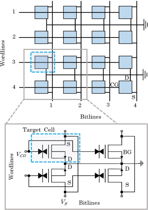
SECTION VI. Memory ArchitecturesThe similarities between the device reported here and Flash memory cells readily allow compatibility with Flash architectures, i.e., it could be implemented in a NAND-type architecture, with devices connected in series in large strings. This will allow for a low-power high-endurance alternative to NAND Flash. However, large-scale use would require 3-D implementation and consequent increase in areal bit density to compete with the transition from planar to 3-D NAND Flash. An alternative is use in niche applications, where reliable data retention, high speed, and low energy are preferred to the high-bit density of FGMOSFET-based Flash memory. More interesting is the implementation in an architecture suitable for active memory (RAM). The most important feature of an active memory is that it allows fast access to individual bits (devices) at the command of the user [21]. For our devices, this can be realized by implementing a NOR-type architecture (see Fig. 4). Note that we introduce a new device symbol in Fig. 4, similar to the well-known FGMOSFET device symbol but combined with an RT diode symbol to specify the write/erase mechanism. Due to the nature of RT, the current peaks for the write and erase processes are very sharp [see Fig. 1(f)]. This allows for the use of half-voltages, where half of the required voltage for writing or erasing data is applied to the CG and the other half to the channel. When only a single half-voltage is applied to any device, the state of the device remains intact. This feature can be used to target individual devices in an array by selecting half-voltages on the desired wordline and bitline, which we designate as CG and S, respectively. These combine to write or erase the target device without compromising the data stored in the surrounding devices (disturb). It is important to note that the BG terminal serves as a common ground for all devices in the array and that devices are back to back in pairs with grounded drain contacts, permitting a highly efficient architecture (see Fig. 4).
The read operation is otherwise identical to that found in NOR-Flash memory and permits the reading of individual devices with this architecture [22]. This is achieved by applying a read voltage, VREF
, between CG and BG (CG and ground), to the appropriate wordline, a small voltage, e.g., < 0.5 V, to the appropriate bitline, and testing for channel conductivity (current flow). Note that since the devices are normally off, current will only flow if the particular device that is addressed is in a logical-1 state. VREF
should be chosen such that it falls between the two threshold voltages of the 0 and 1 states, e.g., 0.6 V [see Fig. 2(c)]. The ability to target individual devices (bits) lends itself toward RAM applications due to the speed of addressing an individual bit at random. Unlike the dominant RAM technology, DRAM, this memory will be nonvolatile with nondestructive read, but with similar (or improved) performance capabilities in other respects.
SECTION VII. Fast Low-Energy NVRAMThe modeling indicates that such an NVRAM can operate at low voltage, low energy, and high speeds. A transient simulation for the write cycle with a 5-ns rise time and 5-ns duration, demonstrating the potential speed of the device, is shown in Fig. 5(a). This gives a total pulse time of 10 ns, similar to the speed of DRAM [23]. There is a dependence on both the rise time and duration of pulse for the threshold shift; thus, they were set equal for the purposes of investigating the device speed. The 5-ns rise-time voltage pulse was selected specifically with DRAM in mind, where this speed limitation is a result of capacitive charging within a memory array. Thus, the choice of the voltage pulse considers capacitive limitations brought about by implementation in a hypothetical array. The figure depicts the change in the threshold voltage in real time during the pulse, along with the corresponding tunneling current density, i.e., the current density tunneling into the FG during the write pulse [see Fig. 5(a)]. The charge density stored in the FG is, therefore, the area under this plot and is the sole reason for the change in the threshold voltage in accordance with (1). Fig. 5(b) shows the same plot for the erase cycle, operating at similar speed and voltage, although not exactly the same, as the voltages have been optimized for minimal disturbances and an exact return to the original state after the erase cycle, i.e., with equal area under the current density curves (see Fig. 5), as we discuss now.
The four optimized half-voltage pulses are −0.85 V (CG-write), 0.90 V (S-write), −1.16 V (S-erase), and 1.16 V (CG-erase). The total voltage for the write and erase cycles is slightly larger than the voltages corresponding to the peak current density [see Fig. 1(e)]. This is due to the change in voltage on VFG1
during the write and erase processes, which screens some of the applied potential and must be compensated by a slightly higher voltage. The unique voltage amplitude to each bitline or wordline for write or erase is chosen such that the threshold shift for the write and erase processes is exactly opposite, ensuring there is no drift in the threshold voltages over many cycles. The half-voltages, when applied individually, have a negligible effect on surrounding cells. The greatest disturbance on the cells was from the −0.85-V write half-voltage applied to the wordline and was determined to be approximately one electron loss every 4000 10-ns pulses for a 20-nm feature size. The extremely low disturbance of cells is derived from the lack of tunneling current at low voltages. This is demonstrated directly from the current density simulations [see Fig. 1(f)], where the current density is under 1 Acm−2 in the 0.85–1.16-V range (compared with a 104 Acm−2 peak magnitude). For the read process, the model predicts an excellent 0/1 threshold contrast of 430 mV [see Fig. 2(c)]. If we now compare some of the important memory metrics for different types of memory cells with 20-nm feature size cell [23], [24], both in production and under development, we observe some interesting results (see Table II). The most notable is the switching energy, which is lower than both DRAM and 3-D NAND Flash by factors of 100 and 1000, respectively, and thus also significantly lower than other emerging memory technologies. This remarkable observation is a result of the combination of low voltages and small capacitance in our devices. Furthermore, it contradicts the argument that nonvolatility requires the expenditure of more energy to change the states than a volatile memory, due to the energy required to overcome the barrier energy [23]. This is not the case for RT as there exists only very specific energy alignments at which the tunneling can occur, allowing us to have a high barrier energy but still observe tunneling at small voltages. The only issue that comes to light in the benchmarking metrics listed in Table II is the electron number, which is the downside of the small capacitance of the FG. With only 100 electrons in the FG for the written state (0) at this feature size, a leakage of 30–50 electrons could result in failure of that data cell. However, the simulated 0-V leakage currents are negligible at 300 K, with an extremely small disturb for half-voltage pulses, as previously discussed. Moreover, 2-D NAND Flash technologies of similar feature size have just 30–50 electrons per cell level [24]. This comparison, combined with the high barrier energy and low disturb rate, suggests that this low number of stored electrons is not a stumbling block, at least until the technology is scaled to feature sizes < 10 nm. We have demonstrated a III-V semiconductor NVRAM with startlingly low switching energy (10−17 J for a 20-nm feature size) that operates as an FG memory at significantly lower voltages than Flash (≤2.3 V). Positive endurance and data retention results are expected due to the extremely low switching energy and large barrier energy (2.1 eV), although rigorous testing of this on experimental devices is required. The combination of nextnano.MSB, nextnano++, and SPICE simulations indicates that the device can operate virtually disturb-free at 10-ns pulse durations, a similar speed to the volatile alternative, DRAM. These advantages are derived from the triple-barrier RT mechanism used to transport the charge in and out of the device, which occurs at much lower voltages than other FG memories (i.e., Flash). The proposed device has a threshold voltage and threshold voltage shift due to charge storage, allowing a similar read process to that of FGMOSFET cells used in Flash memory. This is achieved using a broken gap (Type-III) conduction band alignment formed from an In1-xGaxAs/GaSb heterojunction, where the In1-xGaxAs channel is a thin (12 nm) QW. An excellent contrast in threshold voltages between the 0 state and 1 state is achieved. The resemblance to Flash memory cells allows NAND or NOR Flash architectures to be directly implemented on the device to produce large arrays. The simulation results indicate that half-voltages can be used within a NOR-type architecture to target individual cells for write, erase, and read processes. This exclusive feature, combined with the increased speed suggested from the transient results of the 1-D model, predicts that the device can be implemented in large arrays as a low-power, nonvolatile, nondestructively read alternative to DRAM. ACKNOWLEDGMENTThe data in the figures of this manuscript are openly available from Lancaster University data archive in [27].
|